Pci-pdiso16 block diagram – Measurement Computing PCI-PDISO16 User Manual
Page 9
Advertising
PCI-PDISO16 User's Guide
Introducing the PCI-PDISO16
9
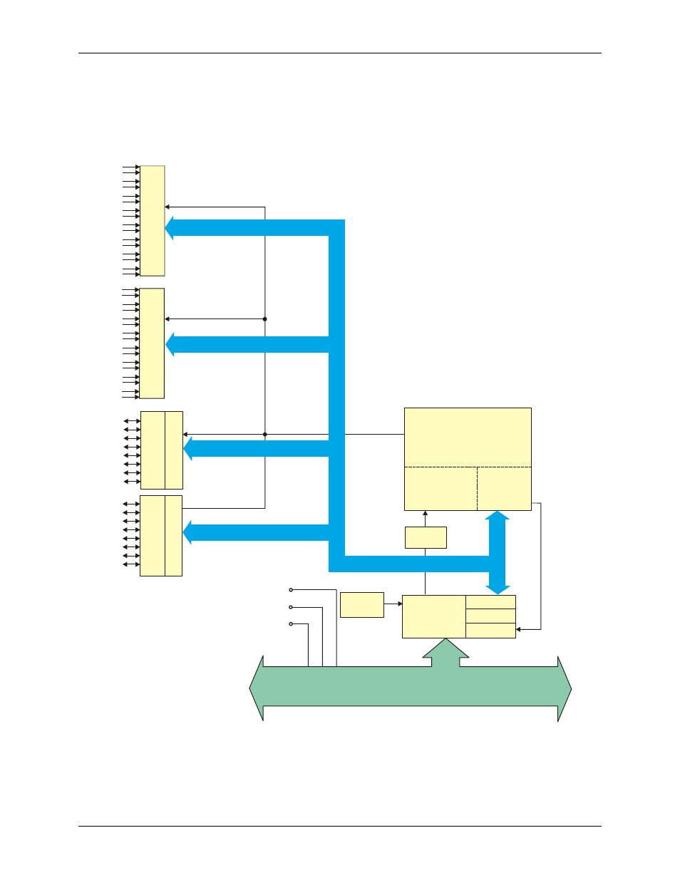
PCI-PDISO16 block diagram
The PCI-PDISO16 provides isolated input channels and relay output channels on each connector. The block
diagram shown here illustrates the board’s functionality.
PCI
CONTROLLER
BADR1
Boot
EEPROM
Control
Registers
Decode/Status
Bus
Timing
Controller FPGA and Logic
Local Bus
PCI Bus (5V, 32-BIT, 33 MHZ)
Control
Bus
C
o
n
tr
o
l
Interrupt
Control
+5V
+12V
-12V
BADR2
Interrupt
C
o
n
tr
o
l
P
o
rt
A
R
e
la
y
s
0
-7
Ip
o
rt
A
I
n
p
u
ts
0
-7
P
o
rt
B
I
n
p
u
ts
0
-7
R
e
la
y
O
u
tp
u
ts
Is
o
la
te
d
I
n
p
u
ts
P
o
rt
B
R
e
la
y
s
0
-7
Figure 1. PCI-PDISO16 functional block diagram
Advertising