Analog isolation applications, Introduction, Basic building blocks for analog isolation – Avago Technologies ACPL-224-500E User Manual
Page 40
AV02-4387EN
37
Avago Technologies
Analog Isolation Applications
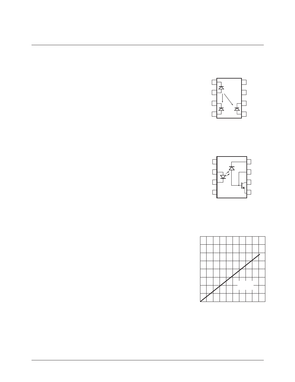
Figure 1. HCNR-200/1 High Linearity Analog
Isolator
Introduction
Optoisolators transfer analog and
digital signals from one circuit
section or module to another in the
presence of a large potential dif-
ference or induced electrical noise
between the ground or common
points of these modules. Examples
of analog isolation applications
are interfaces to: A/D converters,
sensing circuits such as thermocou-
ples and transducers, patient moni-
toring equipment, motor speed
and position measurement circuits,
audio and video amplifiers, and
power supply feedback.
Basic Building Blocks for Analog
Isolation
Avago Technologies’ HCNR200/1 and
HCPL4562 constitute basic optical cou-
pling building blocks for high linearity
isolation applications. Figures 1 and 2
show the respective optical coupling
mechanisms for these two optoisola-
tors. Both these isolators use high-per-
formance AlGaAs LEDs and photodiode
combinations with higher speed and
linearity compared to conventional op-
toisolators. The HCNR200/1 LED illumi-
nates two closely matched photodiodes,
one on the input side, and another on
the output side. With a suitable appli-
cations circuit for the HCNR200/1, the
nonlinearity and drift characteristics of
the LED can be virtually eliminated. The
output photodiode produces a photo-
current that is linearly related to the light
output of the LED. The close matching of
the photodiodes and advanced design
of the package ensure the high linear-
ity and stable gain characteristics of the
optoisolator.
Figure 2. HCPL-4562 High Bandwidth Analog
Isolator
Figure 3. HCPL-4562 Base Photo Current vs.
Input Current
The HCNR200/1 optoisolator can be used
as a basic analog isolation building block
for a wide variety of applications that
require good stability, linearity, band-
width and low cost. The HCNR200/1 is
very flexible and, by appropriate design
of the application circuit, is capable of
operating in many different modes, in-
cluding unipolar, bipolar, ac/dc, invert-
ing and non-inverting.
The HCPL-4562 and HCNW4562 are
recommended for very high band-
width (up to 15 MHz) AC analog
designs. If the output transistor
is biased in the active region, the
current transfer ratio relationship for
the HCPL-4562 can be represented
as:
I
C
= K ( I
F
/ I
FQ
)
n
where I
C
is the collector current; I
F
is the LED input current, I
FQ
is LED
input current at which K is meas-
ured; K is the collector current when
I
F
= I
FQ
; and n is the slope of I
C
vs. I
F
on logarithmic scale.
The exponent n varies with I
F
, but
over some limited range of DI
F
, n can
be regarded as a constant. For ac-
signal applications, the HCPL-4562
can be biased at an appropriate
quiescent current where the ratio of
the incremental photodiode current
to incremental LED current is nearly
constant. Figure 3 shows the linear-
ity characteristics of the HCPL-4562.
8
7
6
1
3
HCNR200/1
5
2
4
LED
NC
NC
PD1 PD2
K1
K2
8 V
CC
7 V
B
6 V
O
5 GND
NC
ANODE
CATHODE
NC
1
2
3
4
80
70
60
50
40
30
20
10
0
0
2
0
18
16
14
12
10
8
6
4
2
I
F
- INPUT CURRENT - mA
I
PB
- BASE PHOTO CURRENT -
µA
T
A
= 25
°C
V
PB
> 5 V
HCPL-4562
- ACPL-227-500E ACPL-244-500E ACPL-247-500E ACPL-785J-000E ACPL-C780-000E ACPL-C784-000E ACPL-C78A-000E HCPL-0201 HCPL-0211 HCPL-0300 HCPL-0302 HCPL-0314 HCPL-0370 HCPL-0452 HCPL-0453 HCPL-0454 HCPL-0466 HCPL-0500 HCPL-0501 HCPL-050L HCPL-0530 HCPL-0531 HCPL-0534 HCPL-053L HCPL-0600 HCPL-0601 HCPL-060L HCPL-0611 HCPL-061A HCPL-061N HCPL-0630 HCPL-0631 HCPL-063A HCPL-063L HCPL-063N HCPL-0661 HCPL-0700 HCPL-0701 HCPL-0708 HCPL-070A HCPL-070L HCPL-0710 HCPL-0720 HCPL-0721 HCPL-0723 HCPL-0730 HCPL-0731 HCPL-0738 HCPL-073A HCPL-073L HCPL-0872 HCPL-0900 HCPL-090J HCPL-091J HCPL-092J HCPL-0930 HCPL-0931 HCPL-177K HCPL-177k#200 HCPL-177K-100 HCPL-177K-300 HCPL-177K-600 HCPL-181-000E HCPL-1930 HCPL-1930#100 HCPL-1930#200 HCPL-1930#300 HCPL-1931 HCPL-1931#100 HCPL-1931#200 HCPL-1931#300 HCPL-193K HCPL-193K#200 HCPL-2200 HCPL-2201 HCPL-2202 HCPL-2211 HCPL-2212 HCPL-2219 HCPL-2231 HCPL-2232 HCPL-2300 HCPL-2400 HCPL-2430 HCPL-2502 HCPL-2503 HCPL-250L HCPL-2530 HCPL-2531 HCPL-2533 HCPL-253L HCPL-257K HCPL-257K#200 HCPL-257K-100 HCPL-257K-300 HCPL-2601 HCPL-2602 HCPL-260L HCPL-2611 HCPL-2612 HCPL-261A HCPL-261N HCPL-2630 HCPL-2631 HCPL-263A HCPL-263L HCPL-263N HCPL-268K HCPL-268K#200 HCPL-268K-100 HCPL-268K-300 HCPL-270L HCPL-2730 HCPL-2731 HCPL-273L HCPL-3020 HCPL-3120 HCPL-3140 HCPL-314J HCPL-3150 HCPL-315J HCPL-316J HCPL-3180 HCPL-354-000E HCPL-3700 HCPL-3760 HCPL-4100 HCPL-4200 HCPL-4502 HCPL-4503 HCPL-4504 HCPL-4506 HCPL-4534 HCPL-4562 HCPL-4661 HCPL-4701 HCPL-4731 HCPL-5120 HCPL-5120-100 HCPL-5120-200 HCPL-5120-300 HCPL-5121 HCPL-5121-100 HCPL-5121-200 HCPL-5121-300 HCPL-5150 HCPL-5150-100 HCPL-5150-200 HCPL-5150-300 HCPL-5151 HCPL-5151-100 HCPL-5151-200 HCPL-5151-300 HCPL-5200 HCPL-5200#100 HCPL-5200#200 HCPL-5200#300 HCPL-5201 HCPL-5201#100 HCPL-5201#200 HCPL-5201#300 HCPL-520K HCPL-520K#200 HCPL-520K-100 HCPL-520K-300 HCPL-5230 HCPL-5230#100 HCPL-5230#200 HCPL-5230#300 HCPL-5231 HCPL-5231#100 HCPL-5231#200 HCPL-5231#300 HCPL-523K HCPL-523K#200 HCPL-523K-100 HCPL-523K-300 HCPL-5300 HCPL-5300#100 HCPL-5300#200 HCPL-5300#300 HCPL-5301 HCPL-5301#100 HCPL-5301#200 HCPL-5301#300 HCPL-530K HCPL-530K#200 HCPL-5400 HCPL-54#100 HCPL-54#200 HCPL-54#300 HCPL-5401 HCPL-5401#100 HCPL-5401#200 HCPL-5401#300 HCPL-540K HCPL-540K#200 HCPL-540K-100 HCPL-540K-300 HCPL-5430 HCPL-5430#100 HCPL-5430#200 HCPL-5430#300 HCPL-5431 HCPL-5431#100 HCPL-5431#200 HCPL-5431#300 HCPL-543K HCPL-543K#200 HCPL-543K-100 HCPL-543K-300 HCPL-5500 HCPL-5500#100 HCPL-5500#200 HCPL-5500#300 HCPL-5501 HCPL-5501#100 HCPL-5501#200 HCPL-5501#300 HCPL-550K HCPL-550K#200 HCPL-550K-100 HCPL-550K-300 HCPL-5530 HCPL-5530#100 HCPL-5530#200 HCPL-5530#300 HCPL-5531 HCPL-5531#100 HCPL-5531#200 HCPL-5531#300 HCPL-553K HCPL-553K#200 HCPL-553K#300 HCPL-553K-100 HCPL-5600 HCPL-5600#100 HCPL-5600#200 HCPL-5600#300 HCPL-5601 HCPL-5601#100 HCPL-5601#200 HCPL-5601#300 HCPL-560K HCPL-560K#200 HCPL-560K-300 HCPL-560K-100 HCPL-5630 HCPL-5630#100 HCPL-5630#200 HCPL-5630#300 HCPL-5631 HCPL-5631#100 HCPL-5631#200 HCPL-5631#300 HCPL-563K HCPL-563K#200 HCPL-563K-100 HCPL-563K-300 HCPL-5650 HCPL-5650#200 HCPL-5651 HCPL-5651#200 HCPL-5700 HCPL-5700#100 HCPL-5700#200 HCPL-5700#300 HCPL-5701 HCPL-5701#100 HCPL-5701#200 HCPL-5701#300 HCPL-570K HCPL-570K#200 HCPL-570K#300 HCPL-570K-100 HCPL-5730 HCPL-5730#100 HCPL-5730#200 HCPL-5730#300 HCPL-5731 HCPL-5731#100 HCPL-5731#200 HCPL-5731#300 HCPL-573K HCPL-573K#200 HCPL-573K#300 HCPL-573K-100 HCPL-5760 HCPL-5760#100 HCPL-5760#200 HCPL-5760#300 HCPL-5761 HCPL-5761#100 HCPL-5761#200 HCPL-5761#300 HCPL-576K HCPL-576K#200 HCPL-576K-100 HCPL-6230 HCPL-6231 HCPL-623K HCPL-6250 HCPL-6251 HCPL-625K HCPL-6430 HCPL-6431 HCPL-643K HCPL-6530 HCPL-6531 HCPL-653K HCPL-6550 HCPL-6551 HCPL-655K HCPL-6630 HCPL-6631 HCPL-663K HCPL-6650 HCPL-6651 HCPL-665K HCPL-6730 HCPL-6731 HCPL-673K HCPL-6750 HCPL-6751 HCPL-675K HCPL-7510 HCPL-7520 HCPL-7560 HCPL-7710 HCPL-7720 HCPL-7721 HCPL-7723 HCPL-7800 HCPL-7800A HCPL-7840 HCPL-7850 HCPL-7850#100 HCPL-7850#200 HCPL-7850#300 HCPL-7851 HCPL-7851#100 HCPL-7851#200 HCPL-7851#300 HCPL-7860 HCPL-786J HCPL-788J HCPL-814-000E HCPL-817-000E HCPL-9000 HCPL-900J HCPL-901J HCPL-902J HCPL-9030 HCPL-9031 HCPL-J312 HCPL-J314 HCPL-J454 HCPL-J456 HCPL-M452 HCPL-M453 HCPL-M454 HCPL-M456 HCPL-M600 HCPL-M601 HCPL-M611 HCPL-M700 HCPL-M701 HCPL-T250 HCPL-T251