Motor control applications, Ipm dead time and propagation delay specifications – Avago Technologies ACPL-224-500E User Manual
Page 49
AV02-4387EN
46
Avago Technologies
IPM Dead Time and Propagation Delay Specifications
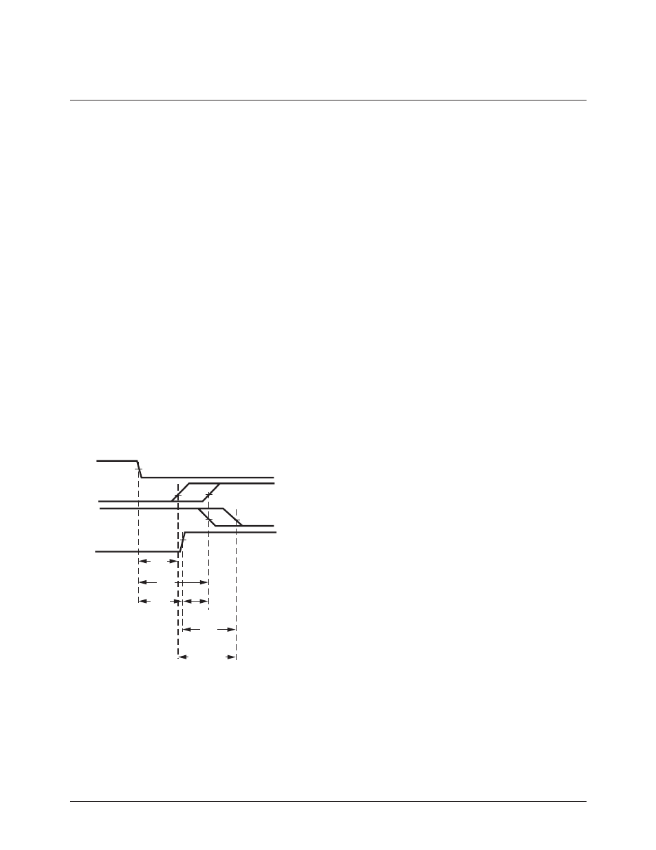
Figure 3. Propagation Delay and Dead Time
analyzed in the same way) it is im-
portant to know the minimum and
maximum turn-on (t
PHL
) and turn-
off (t
PLH
) propagation delay specifi-
cations, preferably over the desired
operating temperature range.
The limiting case of zero dead time
occurs when the input to Q1 turns
off at the same time that the input
to Q2 turns on. This case determines
the minimum delay between LED
1
turn-off and LED
2
turn-on, which is
related to the worst case optocou-
pler propagation delay waveforms,
as shown in Figure 3. A minimum
dead time of zero is achieved in
Figure 3 when the signal to turn on
LED
2
is delayed by (t
PLH max
- t
PHL min
)
from the LED
1
turn off. Note that the
propagation delays used to calcu-
late PDD are taken at equal temper-
atures since the optocouplers under
Motor Control Applications
Many of Avago’s gate drive and IPM
interface optocouplers include a
Propagation Delay Difference (PDD)
specification intended to help de-
signers minimize “dead time” in their
power inverter designs. Dead time is
the time periods during which both
the high and low side power transis-
tors (Q
1
and Q
2
) of a power module
are off. Any overlap in Q
1
and Q
2
con-
duction will result in large currents
flowing through the power devices
between the high and low voltage
motor rails.
To minimize dead time the design-
er must consider the propagation
delay characteristics of the optocou-
pler as well as the characteristics of
the IGBT gate drive circuit. Consider-
ing only the delay characteristics of
the optocoupler (the characteristics
of the IGBT gate drive circuit can be
consideration are typically mounted
in close proximity to each other.
(Specifically, t
PLH max
and t
PHLmin
in
the Figure 3 equations are not the
same as the t
PLH max
and t
PHL min
,
over the full operating temperature
range, specified in the data sheet.).
This delay is the maximum value
for the propagation delay differ-
ence specification that is specified
at 450 ns for the HCPL-4506 over
an operating temperature range of
-40°C to +100°C. Delaying the LED
signal by the maximum propaga-
tion delay difference ensures that
the minimum dead time is zero, but
it does not tell a designer what the
maximum dead time will be. The
maximum dead time occurs in the
highly unlikely case where one op-
tocoupler with the fastest t
PLH
and
another with the slowest t
PHL
are in
the same inverter leg. The maximum
dead time in this case becomes the
sum of the spread in the t
PLH
and
t
PHL
propagation delays as shown in
Figure 3.
The maximum dead time is also
equivalent to the difference between
the maximum and minimum propa-
gation delay difference specifica-
tions. The maximum dead time
(due to the optocouplers) for the
HCPL-4506 is 600 ns over an operat-
ing temperature range of -40°C to
+100°C.
t
PHL
MIN.
I
LED2
I
LED1
V
OUT1
V
OUT2
t
PLH
MIN.
t
PLH
MAX.
t
PHL
MAX.
PDD*
MAX.
MAX.
DEAD TIME
Q1 ON
Q2 OFF
Q2 ON
Q1 OFF
MAXIMUM DEAD TIME (DUE TO OPTOCOUPLER)
= (t
PLH MAX.
- t
PLH MIN.
) + (t
PHL MAX.
- t
PHL MIN.
)
= (t
PLH MAX.
- t
PHL MIN.
) + (t
PLH MIN.
- t
PHL MAX.
)
= PDD* MAX. - PDD* MIN.
PROPAGATION DELAY DIFFERENCE (PPD) MAX.
= (t
PLH
- t
PHL
) MAX. = (t
PLH MAX.
- t
PHL MIN.
)
NOTE: THE PROPAGATION DELAYS USED TO CALCULATE THE
PDD AND MAXIMUM DEAD TIME ARE TAKEN AT EQUAL TEMPERATURES.
- ACPL-227-500E ACPL-244-500E ACPL-247-500E ACPL-785J-000E ACPL-C780-000E ACPL-C784-000E ACPL-C78A-000E HCPL-0201 HCPL-0211 HCPL-0300 HCPL-0302 HCPL-0314 HCPL-0370 HCPL-0452 HCPL-0453 HCPL-0454 HCPL-0466 HCPL-0500 HCPL-0501 HCPL-050L HCPL-0530 HCPL-0531 HCPL-0534 HCPL-053L HCPL-0600 HCPL-0601 HCPL-060L HCPL-0611 HCPL-061A HCPL-061N HCPL-0630 HCPL-0631 HCPL-063A HCPL-063L HCPL-063N HCPL-0661 HCPL-0700 HCPL-0701 HCPL-0708 HCPL-070A HCPL-070L HCPL-0710 HCPL-0720 HCPL-0721 HCPL-0723 HCPL-0730 HCPL-0731 HCPL-0738 HCPL-073A HCPL-073L HCPL-0872 HCPL-0900 HCPL-090J HCPL-091J HCPL-092J HCPL-0930 HCPL-0931 HCPL-177K HCPL-177k#200 HCPL-177K-100 HCPL-177K-300 HCPL-177K-600 HCPL-181-000E HCPL-1930 HCPL-1930#100 HCPL-1930#200 HCPL-1930#300 HCPL-1931 HCPL-1931#100 HCPL-1931#200 HCPL-1931#300 HCPL-193K HCPL-193K#200 HCPL-2200 HCPL-2201 HCPL-2202 HCPL-2211 HCPL-2212 HCPL-2219 HCPL-2231 HCPL-2232 HCPL-2300 HCPL-2400 HCPL-2430 HCPL-2502 HCPL-2503 HCPL-250L HCPL-2530 HCPL-2531 HCPL-2533 HCPL-253L HCPL-257K HCPL-257K#200 HCPL-257K-100 HCPL-257K-300 HCPL-2601 HCPL-2602 HCPL-260L HCPL-2611 HCPL-2612 HCPL-261A HCPL-261N HCPL-2630 HCPL-2631 HCPL-263A HCPL-263L HCPL-263N HCPL-268K HCPL-268K#200 HCPL-268K-100 HCPL-268K-300 HCPL-270L HCPL-2730 HCPL-2731 HCPL-273L HCPL-3020 HCPL-3120 HCPL-3140 HCPL-314J HCPL-3150 HCPL-315J HCPL-316J HCPL-3180 HCPL-354-000E HCPL-3700 HCPL-3760 HCPL-4100 HCPL-4200 HCPL-4502 HCPL-4503 HCPL-4504 HCPL-4506 HCPL-4534 HCPL-4562 HCPL-4661 HCPL-4701 HCPL-4731 HCPL-5120 HCPL-5120-100 HCPL-5120-200 HCPL-5120-300 HCPL-5121 HCPL-5121-100 HCPL-5121-200 HCPL-5121-300 HCPL-5150 HCPL-5150-100 HCPL-5150-200 HCPL-5150-300 HCPL-5151 HCPL-5151-100 HCPL-5151-200 HCPL-5151-300 HCPL-5200 HCPL-5200#100 HCPL-5200#200 HCPL-5200#300 HCPL-5201 HCPL-5201#100 HCPL-5201#200 HCPL-5201#300 HCPL-520K HCPL-520K#200 HCPL-520K-100 HCPL-520K-300 HCPL-5230 HCPL-5230#100 HCPL-5230#200 HCPL-5230#300 HCPL-5231 HCPL-5231#100 HCPL-5231#200 HCPL-5231#300 HCPL-523K HCPL-523K#200 HCPL-523K-100 HCPL-523K-300 HCPL-5300 HCPL-5300#100 HCPL-5300#200 HCPL-5300#300 HCPL-5301 HCPL-5301#100 HCPL-5301#200 HCPL-5301#300 HCPL-530K HCPL-530K#200 HCPL-5400 HCPL-54#100 HCPL-54#200 HCPL-54#300 HCPL-5401 HCPL-5401#100 HCPL-5401#200 HCPL-5401#300 HCPL-540K HCPL-540K#200 HCPL-540K-100 HCPL-540K-300 HCPL-5430 HCPL-5430#100 HCPL-5430#200 HCPL-5430#300 HCPL-5431 HCPL-5431#100 HCPL-5431#200 HCPL-5431#300 HCPL-543K HCPL-543K#200 HCPL-543K-100 HCPL-543K-300 HCPL-5500 HCPL-5500#100 HCPL-5500#200 HCPL-5500#300 HCPL-5501 HCPL-5501#100 HCPL-5501#200 HCPL-5501#300 HCPL-550K HCPL-550K#200 HCPL-550K-100 HCPL-550K-300 HCPL-5530 HCPL-5530#100 HCPL-5530#200 HCPL-5530#300 HCPL-5531 HCPL-5531#100 HCPL-5531#200 HCPL-5531#300 HCPL-553K HCPL-553K#200 HCPL-553K#300 HCPL-553K-100 HCPL-5600 HCPL-5600#100 HCPL-5600#200 HCPL-5600#300 HCPL-5601 HCPL-5601#100 HCPL-5601#200 HCPL-5601#300 HCPL-560K HCPL-560K#200 HCPL-560K-300 HCPL-560K-100 HCPL-5630 HCPL-5630#100 HCPL-5630#200 HCPL-5630#300 HCPL-5631 HCPL-5631#100 HCPL-5631#200 HCPL-5631#300 HCPL-563K HCPL-563K#200 HCPL-563K-100 HCPL-563K-300 HCPL-5650 HCPL-5650#200 HCPL-5651 HCPL-5651#200 HCPL-5700 HCPL-5700#100 HCPL-5700#200 HCPL-5700#300 HCPL-5701 HCPL-5701#100 HCPL-5701#200 HCPL-5701#300 HCPL-570K HCPL-570K#200 HCPL-570K#300 HCPL-570K-100 HCPL-5730 HCPL-5730#100 HCPL-5730#200 HCPL-5730#300 HCPL-5731 HCPL-5731#100 HCPL-5731#200 HCPL-5731#300 HCPL-573K HCPL-573K#200 HCPL-573K#300 HCPL-573K-100 HCPL-5760 HCPL-5760#100 HCPL-5760#200 HCPL-5760#300 HCPL-5761 HCPL-5761#100 HCPL-5761#200 HCPL-5761#300 HCPL-576K HCPL-576K#200 HCPL-576K-100 HCPL-6230 HCPL-6231 HCPL-623K HCPL-6250 HCPL-6251 HCPL-625K HCPL-6430 HCPL-6431 HCPL-643K HCPL-6530 HCPL-6531 HCPL-653K HCPL-6550 HCPL-6551 HCPL-655K HCPL-6630 HCPL-6631 HCPL-663K HCPL-6650 HCPL-6651 HCPL-665K HCPL-6730 HCPL-6731 HCPL-673K HCPL-6750 HCPL-6751 HCPL-675K HCPL-7510 HCPL-7520 HCPL-7560 HCPL-7710 HCPL-7720 HCPL-7721 HCPL-7723 HCPL-7800 HCPL-7800A HCPL-7840 HCPL-7850 HCPL-7850#100 HCPL-7850#200 HCPL-7850#300 HCPL-7851 HCPL-7851#100 HCPL-7851#200 HCPL-7851#300 HCPL-7860 HCPL-786J HCPL-788J HCPL-814-000E HCPL-817-000E HCPL-9000 HCPL-900J HCPL-901J HCPL-902J HCPL-9030 HCPL-9031 HCPL-J312 HCPL-J314 HCPL-J454 HCPL-J456 HCPL-M452 HCPL-M453 HCPL-M454 HCPL-M456 HCPL-M600 HCPL-M601 HCPL-M611 HCPL-M700 HCPL-M701 HCPL-T250 HCPL-T251