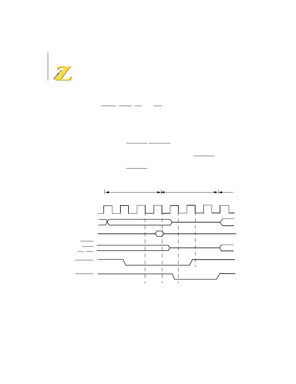
Figure 16. bus exchange timing during memory read – Zilog Z80180 User Manual
Page 41
Z8018x
Family MPU User Manual
26
UM005003-0703
When the bus is released, the address (A0–A19), data (D0–D7), and
control (MREQ, IORQ, RD, and WR) signals are placed in the high
impedance state.
Dynamic RAM refresh is not performed when the Z8X180 has released
the bus. The alternate bus master must provide dynamic memory
refreshing if the bus is released for long periods of time.
Figure 16 illustrates BUSREQ/BUSACK bus exchange during a memory
read cycle. Figure 17 illustrates bus exchange when the bus release is
requested during a Z8X180 CPU internal operation. BUSREQ is sampled
at the falling edge of the system clock prior to T3, T1 and Tx (BUS
RELEASE state). If BUSREQ is asserted Low at the falling edge of the
clock state prior to Tx, another Tx is executed.
Figure 16. Bus Exchange Timing During Memory Read
Phi
A0
–
A19
T1
T1
TX
TX
T3
TW
T2
T1
RD, WR
D0
–
D7
MREQ
IORQ
BUSREQ
BUSACK
CPU memory read cycle
Bus release cycle
CPU cycle